We take a look at AMD’s upcoming Zen 5 CPUs and examine architecture changes and accompanying chipsets
The Highlights
- AMD’s Ryzen 9000 desktop CPUs are codenamed Granite Ridge and use the Zen 5 architecture and AM5 socket
- AMD intends for AM5 to last up to 7 years
- AMD has expanded Zen 5’s execution window by 40% with up to 448 supported OPs
- Release Date: August 15, 2024
Table of Contents
- AutoTOC
Intro
AMD’s Zen 5 CPUs will be launching on August 15. We previously covered the inbound CPUs in the 9000 series, but have more technical details now that AMD has hosted a conference dedicated to the Ryzen 9 9950X, R9 9900X, R7 9700X, and R5 9600X. We already posted a separate video featuring the extreme overclocking team with Bill & Amit hitting several new world records on a 16-core CPU.
AMD’s new features include an on-the-fly memory tuning solution, including memory changes from within Windows and without reboot, a new “Curve Shaper” that builds on top of “Curve Optimizer,” new chipsets, and the Zen 5 architecture itself.
We’ll cover the rest of the news about AMD’s Zen 5 CPUs as we prepare our test benches for the upcoming reviews.
Editor's note: This was originally published on July 18, 2024 as a video. This content has been adapted to written format for this article and is unchanged from the original publication.
Credits
Host, Writing
Steve Burke
Writing
Jeremy Clayton
Camera
Vitalii Makhnovets
Video Editing
Tim Phetdara
Writing, Web Editing
Jimmy Thang
Overview
We’ll get right into the quick facts first – some of this we already covered from AMD’s Computex announcement, but some is new information. Unfortunately we don’t have price information to share at the time of writing.
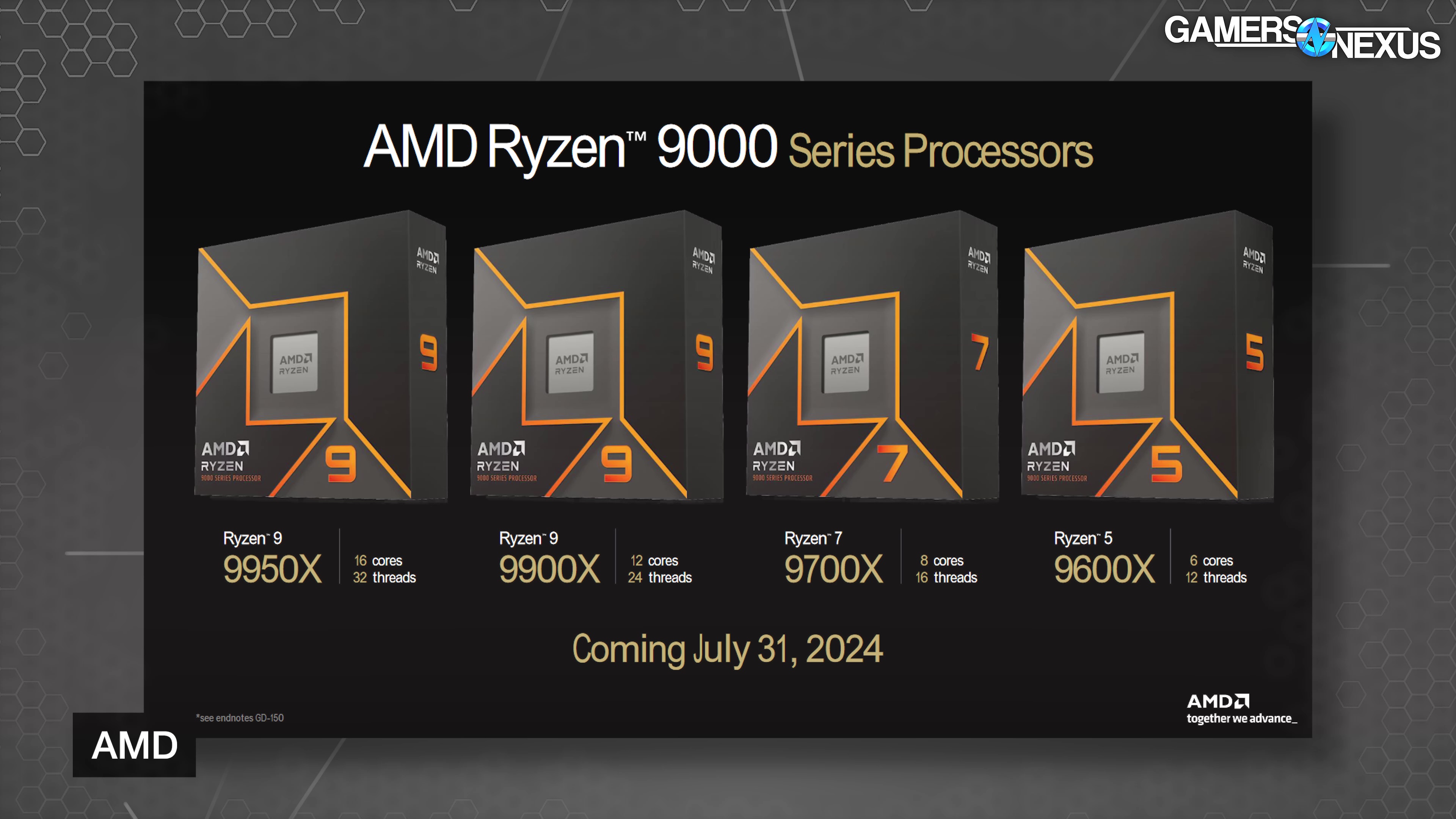
AMD’s Ryzen 9000 desktop CPUs are codenamed Granite Ridge, feature the Zen 5 architecture, and are still on the AM5 socket. This first image will be a recap of things we already knew, followed by new architectural information.
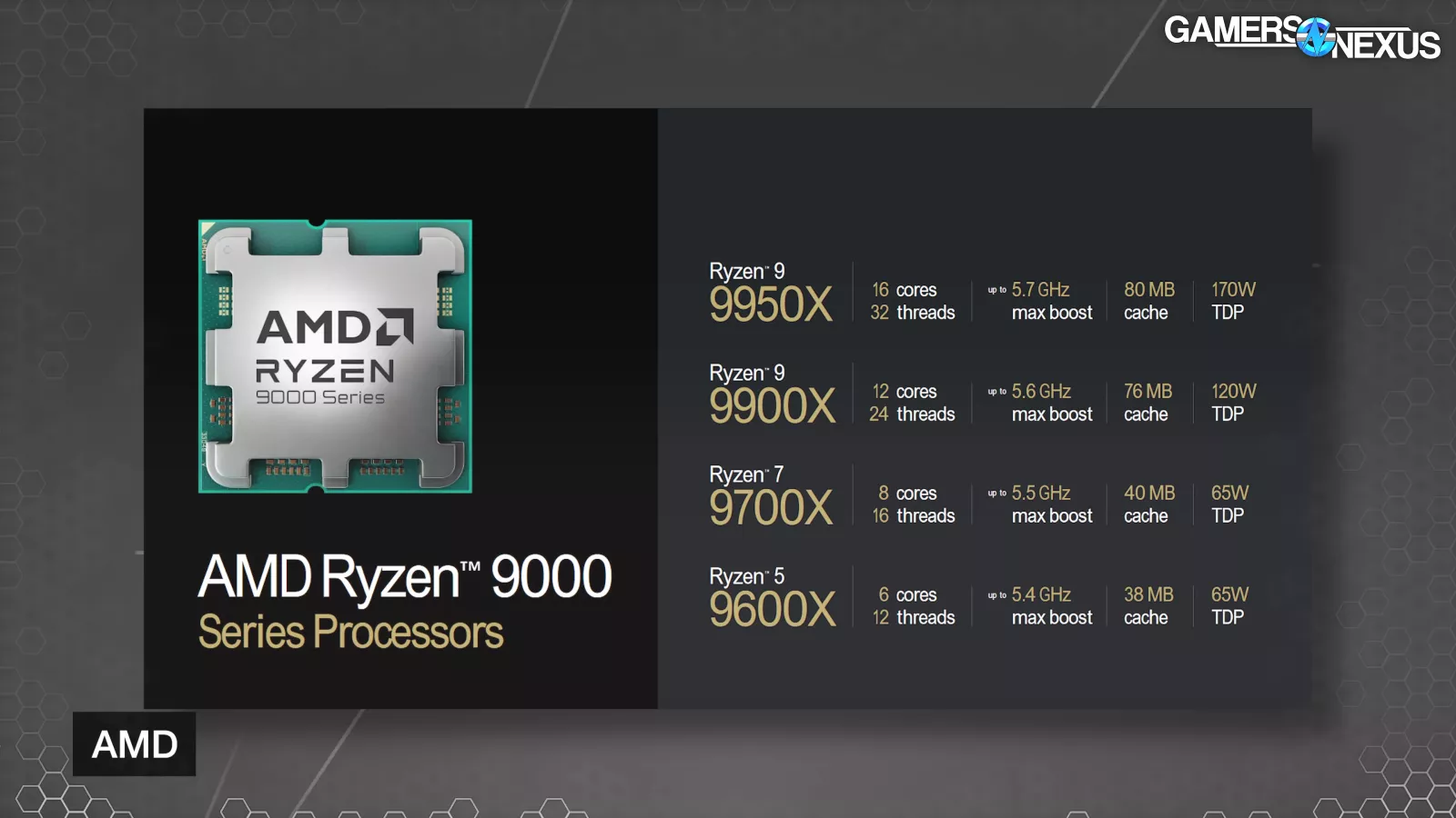
The recap shows that the lineup is fundamentally identical to the initial Ryzen 7000 CPUs. The flagship Ryzen 9 9950X has 16 cores, a 5.7GHz max boost, 80MB of cache, and a 170W TDP. Down from that is the Ryzen 9 9900X with 12 cores, slightly lower boost and cache, and a 120W TDP. Then the Ryzen 7 9700X with 8 cores, 5.5GHz max boost, a smaller 40MB cache due to being single-CCD, and 65W TDP. Finally, the 6-core Ryzen 5 9600X holds up the bottom of the stack.
Notably, the TDPs for the bottom 3 are down significantly versus their Ryzen 7000 counterparts. As a reminder, TDP doesn’t equate to power consumption and isn’t consistent across vendors or even across sockets. AMD’s Package Power Tracking (PPT) is a more useful power consumption guidepost, but we don’t officially have those for Ryzen 9000 yet.
We asked AMD if the TDP formula and HSF thermal resistance values are the same for this series as 7000. AMD confirmed that the comparisons are like-for-like; however, actual power consumption will still vary somewhat. One way that will vary is from reduction in the actual heat, which should reduce power leakage.
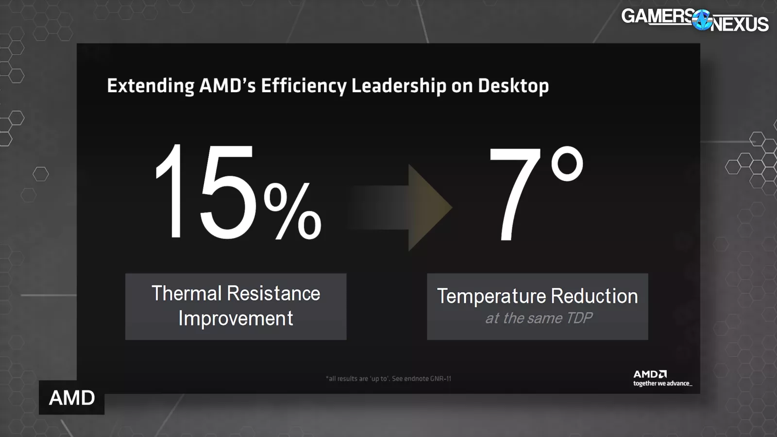
AMD claims it has improved the thermal resistance by 15% for a 7-degree reduction at equivalent TDP. We asked AMD where this improvement came from: The company told us that the improvement is largely from sensor placement optimization, or moving the actual temperature sensors to better locations on the die. This means that the Tdie value will be lower, which AMD says gives it more headroom for boosting.
Zen 5 Architecture
AMD gave press a deeper dive into its architectural changes for Zen 5, and it’s positioning it as a place to grow from.
At the event, AMD CTO Mark Papermaster stated, “It really represents a huge leap forward, and in fact, it’s going to be a pedestal that we’re going to build upon the next several generations of Zen.”
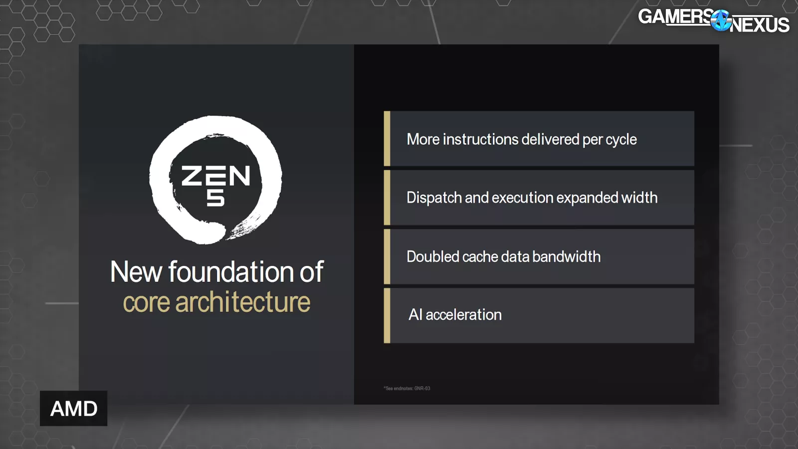
AMD redesigned key elements of the front end, including fetch, decode, and dispatch. This gives more instructions to the back end every clock tick. Zen 5 has wider execution pipelines to execute the instructions. AMD says that efficiency increases from improved cache with more bandwidth and an expanded execution window, which the company states is intended to avoid execution stalls.
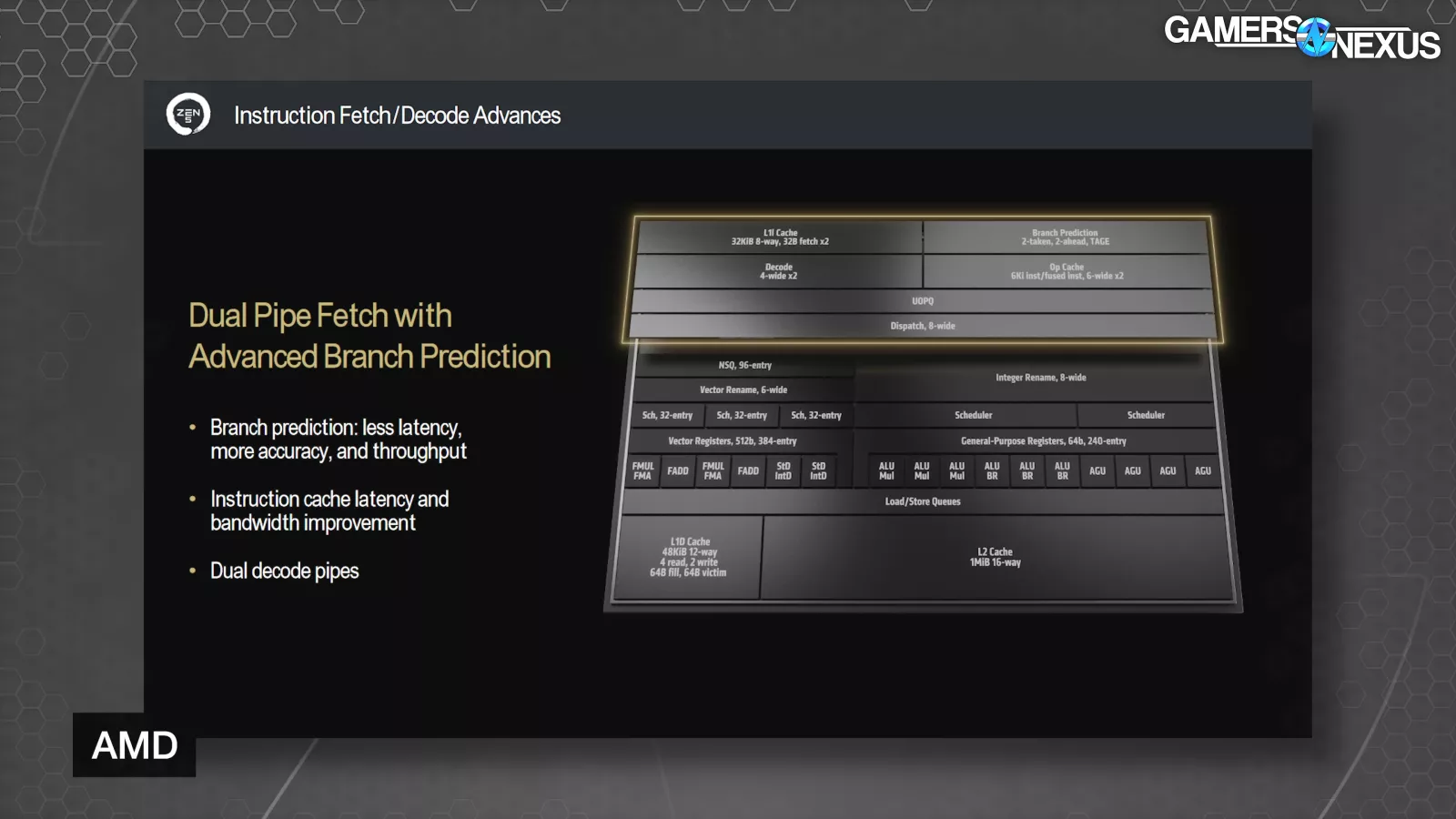
Moving into more detail and starting on the front end with pipe fetch, branch prediction is lower latency, more accurate, and with more predictions per cycle in Zen 5, according to AMD. This all adds up to more throughput in the front end. Downstream, Zen 5 has dual ported instruction cache and op cache, while decreasing latency. AMD also added a dual decode path.
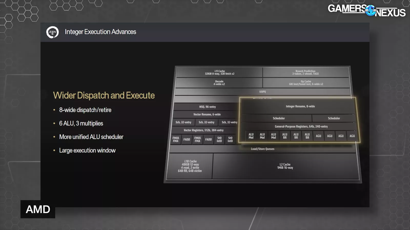
Next is dispatch and the execution engine. Zen 5 features 8-wide dispatch and retire, 6 ALUs with 3 multiplies, and a more unified ALU scheduler (there used to be a unique scheduler for each of the ALUs).
Papermaster went on to say, “We then went from the fact that we had these wider execution pipelines, knowing that when you have more instructions that you're handling, you have to think about handling misses effectively and keeping the performance of those execution pipelines. Again, hardcore micro-architecture engineering.”
AMD also expanded Zen 5’s execution window by 40% with up to 448 supported OPs, which AMD says is a significant driver of more performance. Zen 5 also has a larger 48KB data cache, up from 32KB on Zen4, and double the maximum bandwidth to the L1 cache and Floating-Point Unit, and improved data prefetching.
Papermaster stated, “When you grow caches like that, what typically happens is you run a high risk of increasing the latency. You grew the cache, that's normally going to happen. But what we did in this case, the team just did a phenomenal job. And so they maintained actually that four-cycle access that we had had despite the growth, the 50 percent growth in the data cache. With Zen 5, we can now execute four loads per cycle.”
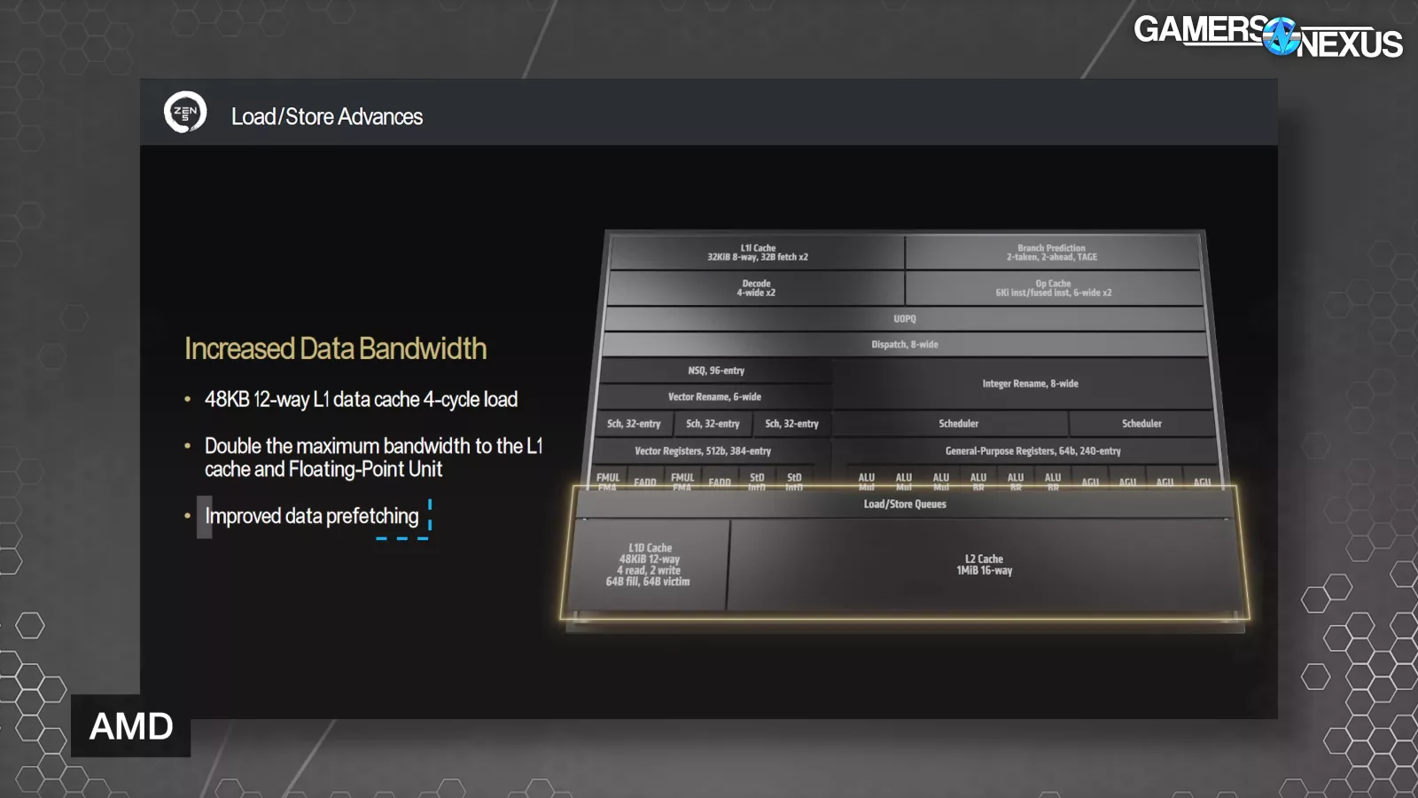
The final key improvement AMD made regarding data bandwidth is to data prefetching, where AMD says that tuned algorithms give much more stride pattern recognition.
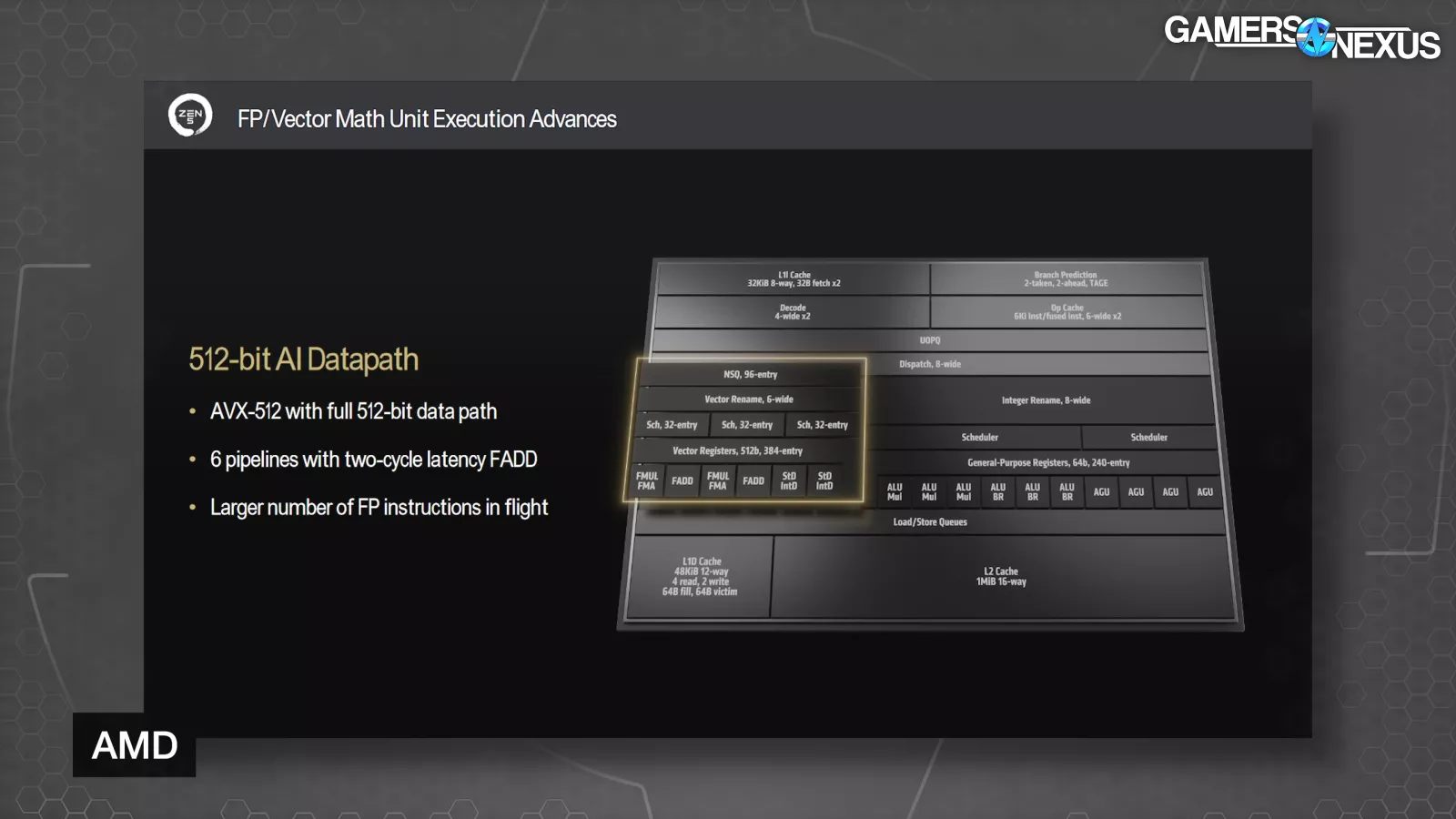
Next are the floating point and vector math unit enhancements. These include a full 512-bit data path, 6 pipelines with two-cycle latency FADD (floating add), and a larger number of floating-point instructions in flight at one time.
Papermaster stated, “So I talked about that 512-bit data path. This is more important than ever. Because when you think about it, there's been no reduction in the kind of math-hungry workloads of gaming, of HPC, of content creation. So when you think about those users of the math unit, none of them are going away. But AI with its need is now becoming a workload everywhere.”
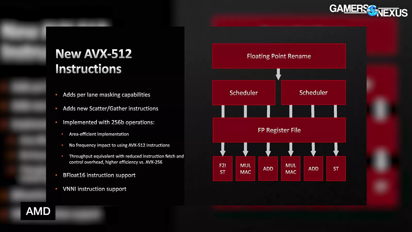
AMD has so far done AVX-512 by double-pumping a 256-bit pipeline, which made sure that the CPU wouldn’t have to drop clocks while doing AVX-512 workloads. With Zen 5, AMD engineered a way to support full frequency while running the physical data path at true 512-bit. Our understanding is that this is modular to the extent that the older double-pump approach is still possible in some situations if the company wants to build it that way.
Zen 5 also lowers the latency of floating-point operations from 3 cycles to 2.
Papermaster stated, “So we doubled the physical pipeline, we lowered the latency, we’ve increased the throughput. And that, combined with the load/store improvements that I described, really create a super optimized engine across those workloads I described – AI, HPC, gaming, content creation.”
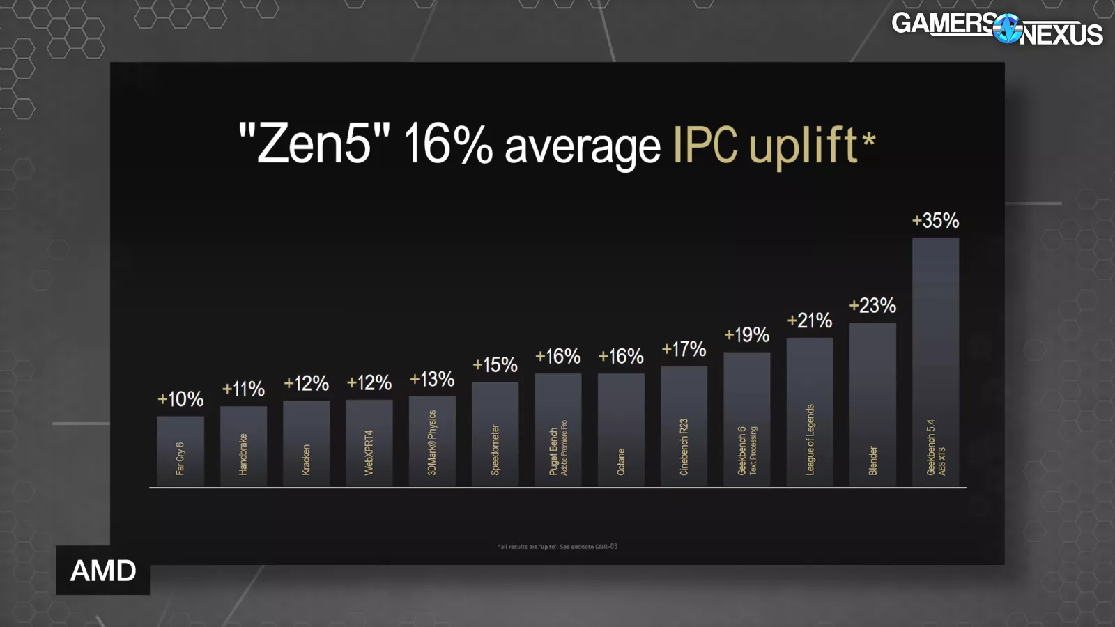
All of these improvements bundled together result in the claimed 16% average geomean uplift in IPC versus Zen 4, with up to 35% single core uplift in AES-XTS encryption.
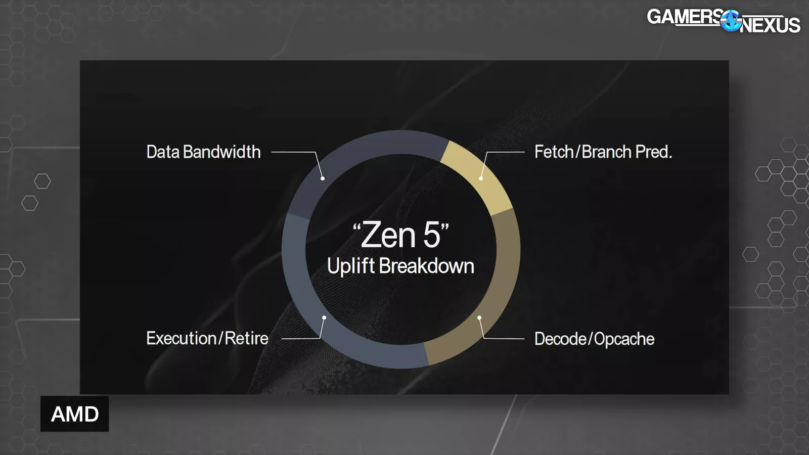
The breakdown of Zen 5’s uplift consists of data bandwidth, fetch/branch prediction, execution/retire, and decode/opcache improvements.
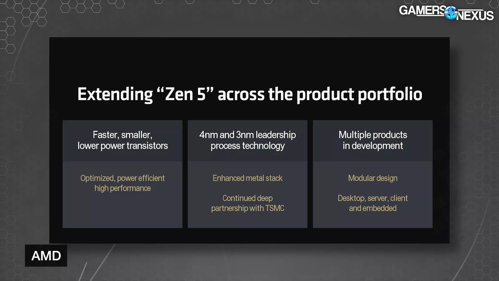
In a more physical sense, Zen 5 moves to 4nm and 3nm process technology with an enhanced metal stack for higher performance and lower resistance.

Ryzen 9000 Performance Claims
AMD shared first-party performance claims that focused on IPC improvements – something AMD wanted to make very clear since the listed max boost frequencies aren’t moving much, if at all. We won’t spend too much time here, since we’ll have our own full testing for each CPU, and it’s never good to blindly trust the manufacturer’s own benchmarks. This will at least set expectations. Our review will run near launch.
According to AMD, the first set of tests were performed with matched clocks between a 9950X and 7700X. Claimed IPC uplift ranged from up to 10% in Far Cry 6, to 23% in Blender. Geekbench 5.4 was even higher, but seems like a potential outlier.
We would have preferred if these were done with matched core counts, as AMD is basically asking us to extend the benefit of the doubt that the tests weren’t set up to give an advantage to the CPU with a physical hardware advantage.
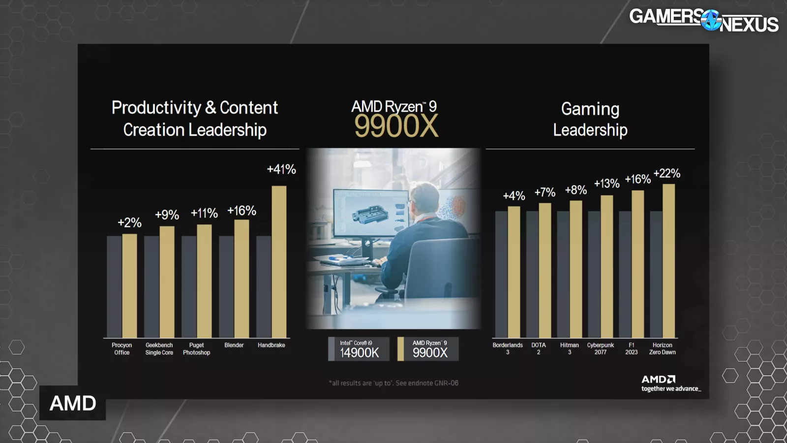
Moving on to AMD’s competitive testing, it matched up the 12-core 9900X versus Intel’s 14900K, claiming a 41% improvement in Handbrake, 22% in Horizon Zero Dawn, and 4% in Borderlands 3.
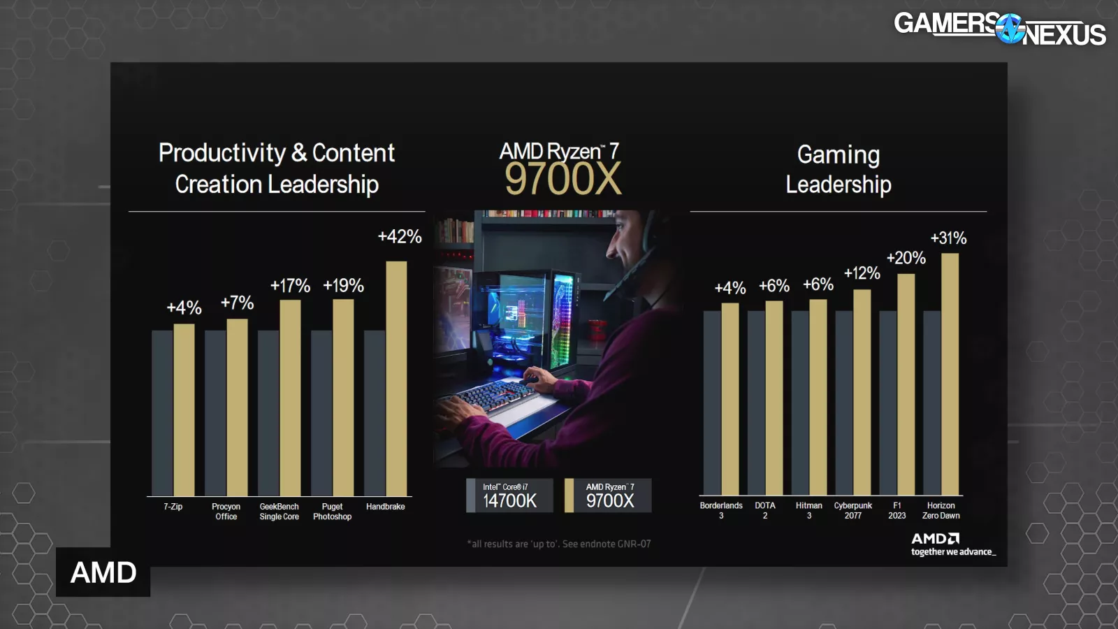
AMD also compared its 9700X to the 14700K, citing a 19% advantage in Puget’s Photoshop benchmark, which we’ll run in our review, and game benchmarks that ranged between 4% and 31% in the 9700X’s favor.
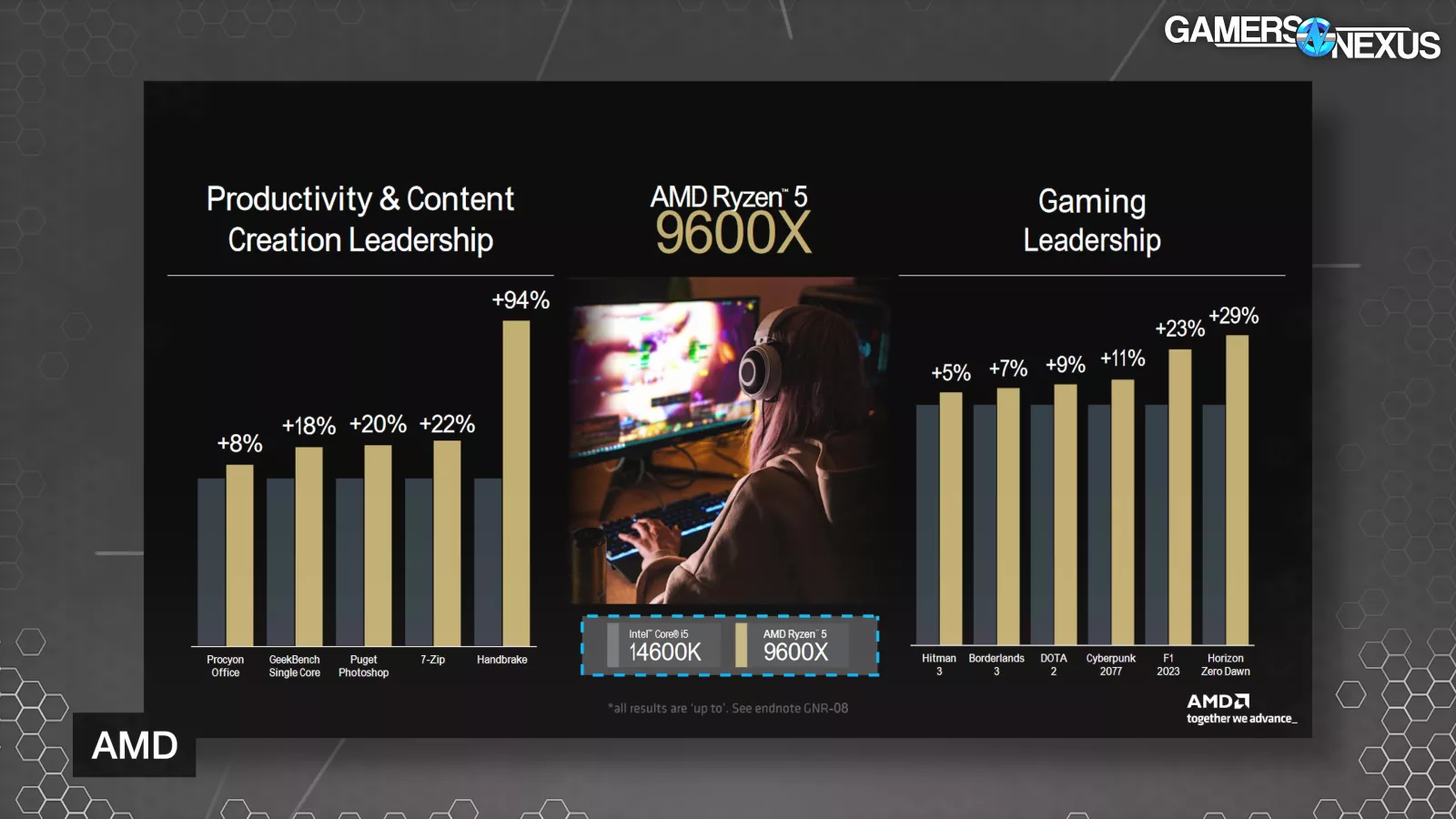
Then finally moving on to the 9600X, AMD matched it against the 14600K. There’s a massive 94% win in Handbrake, along with a smattering of other productivity and gaming wins.
Comparing its former AM4 king, AMD ran the 9700X versus the 5800X3D where it claims an average 12% faster geomean. That could be a huge efficiency win as well, but we’ll need to test it.
AMD SOC Architecture Panel
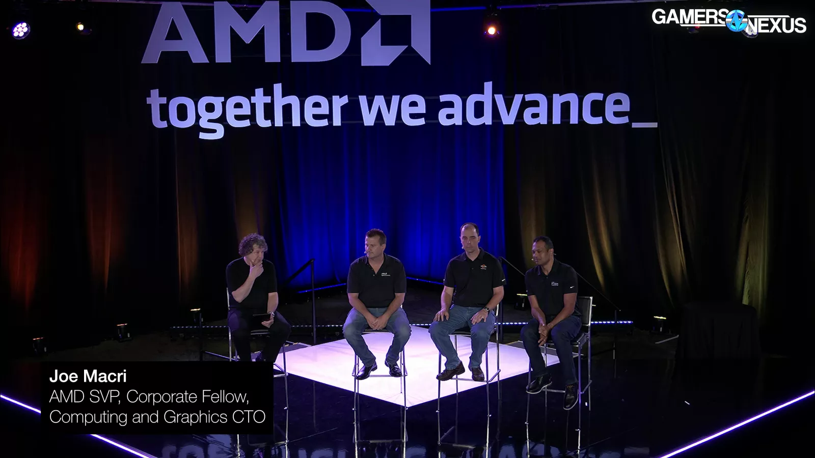
At the end of AMD’s event, it held an SOC architecture panel with four of its Fellows that had some really interesting insights into various aspects of AMD’s design and process and approach. These are four engineers at the company. Mike Clark is the Chief Architect of Zen and its originator, Will Harris is a platform engineer and knows the chipset and socket, Mahesh Subramony is a silicon design engineer, and Joe Macri is the computing & graphics CTO.
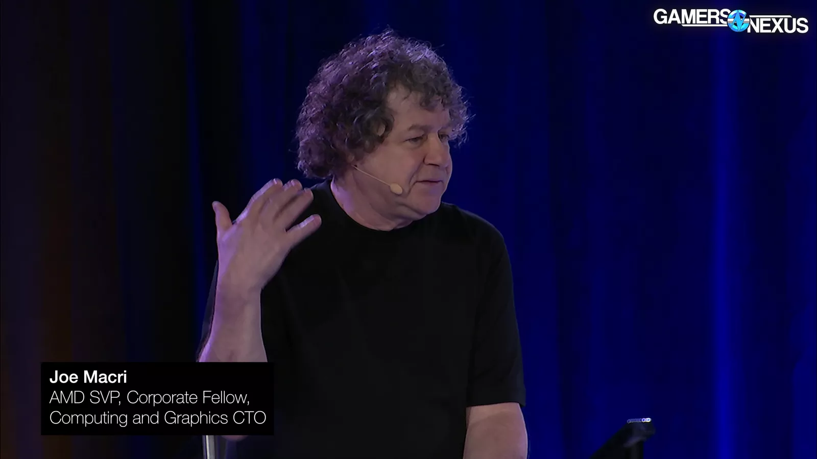
One of the early questions had to do with the fact that AMD is rolling out heterogeneous core architectures in some of its products. There was a funny slip -- or maybe not -- from computing & graphics CTO Joe Macri, “Mahesh, you know, when we look at our competition, Intel, you know, they have a performance core, an economy core.” There were some stifled laughs in the crowd from that one -- it comes across as a dig at what Intel calls the “efficient” core.
Macri also stated, “You know, we have heterogeneous cores also. Our philosophy is different in how we approach desktop or mobile.” Turning to Mahesh Subramony, Macri asked, “Maybe you could, you know, dive in a little bit there and explain, you know, why two companies that are aiming at the same markets approach things just so differently.”
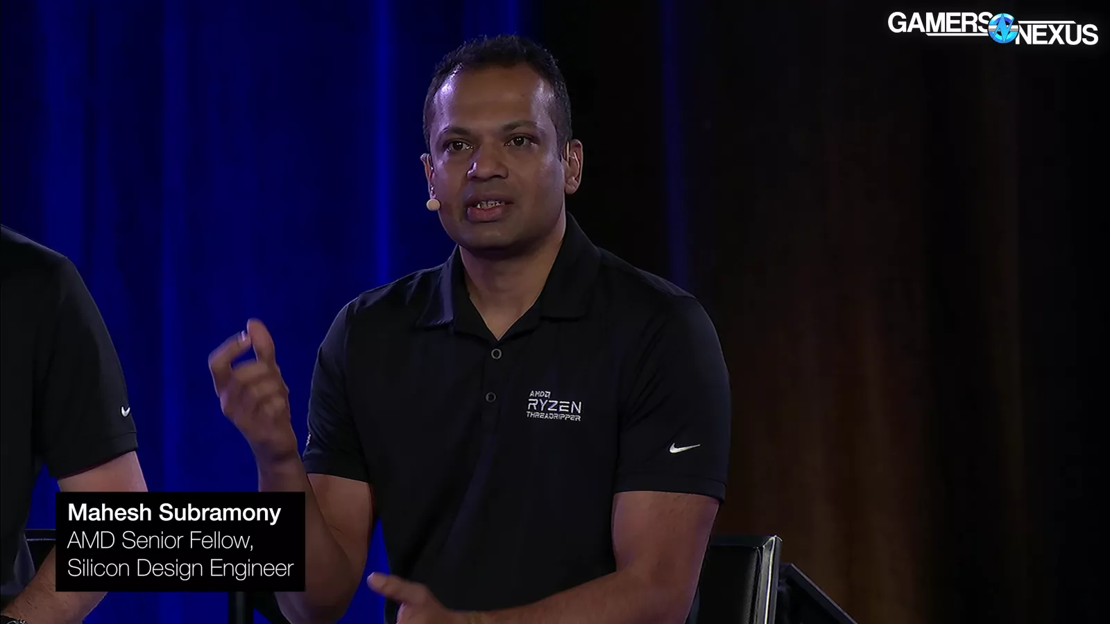
AMD Senior Fellow and Silicon Design Engineer Mahesh Subramony replied, “It really is microarchitecture exact, ISA exact, and IPC exact modular, the cache size it attaches to. So the heterogeneity, if you will, is really around the voltage frequency response. So giving up some of that peak, frequency peak performance and get some of that back in area and efficiency. So that's what the compact core does for us. The desktop user demands performance, low latency and throughput for every task they want to do. So they are better served with a homogenous classic core with a better performance, if you will, and a voltage frequency response, if you will, dynamic. And on the mobile side, even though they are not that far behind in their compute requirements, they care a lot about power efficiency. And that's where the compact core kind of fits right in. A right mix of the classic and the compact cores delivers that scalability in performance without compromising on the power efficiency.”
Macri added that since AMD’s compact cores are in essence the same as regular cores, it makes things easier from an OS software perspective, “The corner cases that you experience when you got cores that are very separate in their attributes just confound the user, make that user experience more difficult, make the OS partners have a more difficult life.”
Those are interesting words from the company that shipped the 7950X3D and 7900X3D – CPUs with different performance characteristics resulting from having one CCD with stacked V-Cache and lower core frequency, and the other without the extra cache but higher core frequency. Those CPUs open up a can of worms that, in order to get the best performance in all circumstances, require special drivers and even user knowledge and intervention that we would classify as confounding.
Macri then addressed AMD Fellow and Platform & Systems Architecture Will Harris, bringing up the AM5 platform, its socket, and longevity – stating that AMD intends for AM5 to last up to 7 years. Will Harris, AMD Fellow of Platform and System Architecture responded by saying, “And so one of the first things that we do as we're designing a new infrastructure, such as AM4, AM5, is we kind of tie it to a major interface that's transitioning. So, in general, it's usually memory, for example. So AM4 was tied with DDR4, and AM5 was tied with DDR5.” Harris added, “...And like you said, we want that longevity, so then we do things like making sure that we have sufficient interfaces to go for several generations. We make sure that we've got the signal integrity, isolation on the pins on the package, so that we can get a few speed bumps and improvement over time on things like memory speeds or PCI Express speeds, for example.”
Harris also said AMD evaluates industry trends, standards committees, and third party vendors to see where the market is heading more long-term.
Subramony then jumped in, saying that with generational gains in the same die area slowing down, AMD has to add die size in order to get more substantial gains in IPC and total performance. If the dies get larger, they still need to fit on the same physical package – a difficult challenge across multiple generations. Macri responded, “And, you know, the team has to dive in at the device physics level, right, the process technology as we shrink it, you know, voltages want to come down, but the platform has to stay consistent.”
Macri took the opportunity to get in another shot at Intel, “You don't have to go change your motherboard every other generation like some other folks do.”
Fair enough, as long as AMD doesn’t start doing that at some point. We’re good to at least 2027, according to AMD.
The conversation then turned to Simultaneous Multi-Threading, or SMT, addressing Intel leaving behind Hyper-Threading on the upcoming P-cores in Lunar Lake.
At the event, AMD Corporate Fellow and Silicon Design Engineer Mike Clark stated, “Yeah, so I think as we talked about heterogeneity earlier, you know, with Intel having two core types, one with SMT and one without, I can definitely see how that would be really hard to manage for software. So I can't really comment more on their design choices, but that seems like an obvious one that sticks out.”
Again, AMD’s 7950X3D is right there staring us in the face with the same scheduling problems, but Clark continued, addressing the actual topic at hand, “For us, I mean, SMT is the best perf per watt per area feature that we have. …Implementation does matter, too, so you have to do it in a very smart way, just like all the microarchitectural features, you know, Mark rolled out yesterday. And so for us, you know, SMT is about a 5 to 10 percent area hit versus, you know, workload improvements that go from 20 to 50 percent.”
Clark then stated that SMT doesn’t work in every scenario, and that if a workload is bandwidth intensive, having more cores won’t help more than having SMT. AMD makes some processors with SMT off, and it allows the end user to turn it off.
They also briefly discussed future Zen 6 and Zen 7 CPUs, but it was limited to the fact that AMD views Zen 5 as the new starting point for the architectures to come, in the same way that Zen 1 was for its subsequent generations.
Chipset Differences
AMD is launching 4 new chipsets in the immediate future: X870E (a 2-die solution), X870, B850, and B840.
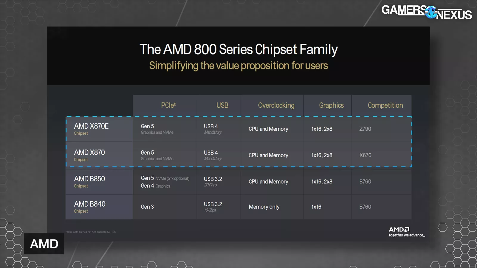
This table simplifies it. AMD’s X870E and X870 chipsets will both run PCIe Gen5 to graphics and NVME. This is a hard requirement, as we understand it, that the motherboard vendors have to follow. Both will also support USB4 as a requirement, CPU and memory overclocking, and run 1x PCIe Gen5 x16 graphics slots or can run 2x 8-lane configurations.
AMD’s X870E chipset will use 2x Promontory 21 dies and keeps the dual-chipset silicon layout of X670E. Everything else uses a single chipset. This allows one of the chipset dies to be closer to the PCIe slots, which can be useful in trace routing. It also expands the general purpose PCIe lane count. B850 drops to Gen4 on the hard requirement for graphics, but can use Gen5 for graphics. USB3.2 at 20Gbps is also required. B840 is effectively an A-series chipset, similar to the prior A320, except rebranded presumably to either trick confusers intentionally or to just cause unnecessary confusion and havoc in the market. This is a low-end chipset that cuts-off at PCIe Gen3, runs USB 3.2 10Gbps, and removes CPU OC support. It also only has 1x16 graphics slots.
The primary difference between X870E, X870, and the prior X670E and X670 boards is USB4 support. There may be other meaningful changes like availability of curve shaper, but some of these details aren’t finalized yet.
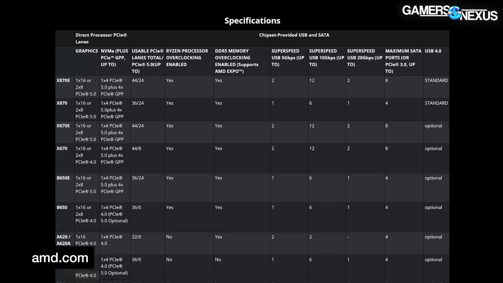
Here’s a full table from AMD.
General Purpose PCIe lanes can be assigned anywhere on the board and are allocated by the motherboard manufacturer, but made available by the chipset. Ryzen CPU combinations with X870E will support up to 44 PCIe lanes, against 36 total on X870. Both support up to 24 PCIe 5.0 lanes. X670E also runs 44 PCIe lanes and 24 up to PCIe 5.0 total. X670 drops to 44 and 8. B850 and B840 aren’t on this table yet.
B840 is effectively an A-series chipset. If you’re going to buy it, just be aware that B840 is not similar to B850 -- it’s a big step down.